Subscribe to get the latest news and updates. No span, we promise.

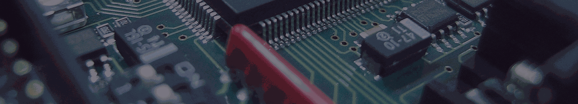
High-speed electronics are now the backbone of modern systems, from aerospace avionics and medical devices to telecommunications infrastructure and AI hardware. However, as signal speeds increase into the GHz range, high speed PCB design noise becomes one of the most critical challenges affecting performance, reliability, and compliance.
In our recent high-speed PCB assembly projects for industrial and embedded applications, one of the most common causes of signal failure, electromagnetic interference, and intermittent operation was excessive on-board noise. Implementing proper pcb noise reduction techniques during the design phase significantly improves signal integrity, reduces EMI risks, and ensures long-term product reliability.
This guide explains the most effective and proven strategies used by modern PCB designers to achieve high speed PCB noise reduction.
Noise in high-speed circuits is primarily caused by unintended electromagnetic interactions between signals, power delivery systems, and PCB layout structures.
|
Noise Source |
Technical Cause |
Impact on PCB |
|
Crosstalk |
Coupling between adjacent traces |
Signal corruption |
|
EMI radiation |
Poor grounding and shielding |
Compliance failure |
|
Power supply noise |
Improper decoupling |
Signal instability |
|
Impedance mismatch |
Incorrect trace design |
Signal reflections |
|
Poor layout |
Long return paths |
Increased interference |
Understanding these sources is the first step toward effective reduce board noise high speed PCBs strategies.
1. Control Crosstalk with Proper Trace Spacing
Crosstalk is one of the most serious signal integrity problems in high-speed circuits. It occurs when electromagnetic energy from one signal trace couples into another.
To achieve effective high speed pcb crosstalk reduction, follow these layout practices:
|
Trace Width |
Minimum Spacing |
|
4 mil |
12 mil |
|
6 mil |
18 mil |
|
8 mil |
24 mil |
These techniques significantly reduce signal coupling and improve overall pcb signal integrity noise performance.
2. Use Continuous Ground Planes for EMI Control
A solid ground plane is essential for pcb emi noise control. It provides a low-impedance return path and reduces electromagnetic radiation.
Best practices include:
Ground Plane Benefits
|
Feature |
Noise Reduction Benefit |
|
Continuous plane |
Reduces EMI radiation |
|
Short return path |
Improves signal integrity |
|
Low impedance |
Stabilizes signals |
Ground planes are one of the most important high speed pcb layout best practices.
3. Implement Proper Decoupling Capacitor Placement
Power supply noise is a major contributor to signal instability.
To achieve effective high speed pcb noise reduction, place decoupling capacitors:
Recommended Decoupling Values
|
Application |
Capacitor Value |
|
High frequency |
0.01 µF |
|
Medium frequency |
0.1 µF |
|
Bulk filtering |
10 µF |
roper decoupling stabilizes voltage and reduces noise propagation.
4. Maintain Controlled Impedance Routing
High-speed signals require controlled impedance to prevent signal reflections and noise.
Design recommendations:
Controlled impedance is essential in high speed pcb design noise control.
5. Optimize PCB Stack-Up Design
Stack-up plays a critical role in noise reduction.
Best stack-up example: Signal, Ground, Power, Signal
Benefits:
This is a core part of reduce board noise high speed PCBs design strategy.
6. Avoid Cold Solder Joints in Assembly
Noise problems are not only caused by design but also by poor assembly.
Cold solder joints can cause:
Prevention methods:
This ensures reliable pcb signal integrity noise performance.
7. Minimize Loop Area
Large current loops act like antennas and radiate noise.
Design recommendations:
This is one of the most overlooked pcb noise reduction techniques.
8. Separate Analog and Digital Circuits
Mixed-signal PCBs are highly sensitive to noise.
Best practice:
This improves overall high speed pcb noise reduction performance.
9. Use Proper Via Design
Poor via design increases impedance and noise.
Recommendations:
This improves signal quality.
Noise directly affects:
Without proper pcb emi noise control, products may fail regulatory testing and experience field failures.
As signal speeds continue to increase, noise control has become one of the most important aspects of modern PCB design. Proper implementation of pcb noise reduction techniques, optimized stack-up, controlled impedance routing, and grounding strategies ensures reliable performance.
Following these proven high speed pcb layout best practices helps engineers successfully reduce board noise high speed PCBs, improve signal integrity, and ensure long-term reliability.
Whether you are designing telecommunications equipment, aerospace electronics, or embedded systems, noise reduction should always be a priority from the initial design stage.