HDI PCB Manufacturer for Fast, Reliable HDI PCB Fabrication & Assembly
Looking for an HDI PCB manufacturer who can deliver precision, fast turnaround, and reliable performance without delays or costly rework? At Sierra Assembly Technology, you get 30+ years of experience, AS9100 Rev-D & ISO 9001:2015 certified processes, and advanced US-based manufacturing all focused on delivering high-quality HDI PCB fabrication and HDI PCB assembly for complex, high-performance applications.
Whether you need a quick HDI PCB prototype or full-scale HDI PCB electronics manufacturing, we help you build smarter, faster, and with complete confidence.
Why Choose Sierra as Your HDI PCB Manufacturer?
-
Faster Time to Market: Tight deadline? Our optimized HDI PCB manufacturing process ensures quick-turn prototypes and production.
-
Lower HDI PCB Cost Without Compromise: We help you reduce unnecessary complexity, minimize rework, and control your HDI PCB cost.
-
High-Density, High-Performance Designs: With advanced high density interconnect PCB capabilities, you can achieve compact, lightweight, and powerful designs.
-
Reduced Risk & Design Errors: Our engineering support helps you identify issues early before they become expensive problems.
-
One Partner for Everything: From HDI PCB fabrication to assembly and testing, we manage the entire process so you don’t have to.
HDI PCB Fabrication & Assembly Built Around Your Needs
1. HDI PCB Fabrication
-
As a leadi-density multilayer boards with microvias, blind/buried vias, and fine trace routing for maximum performance.
2. HDI PCB Assembly
-
Our HDI PCB assembly services ensure precise component placement, strong interconnections, and fully tested boards ready for deployment.
3. HDI PCB Prototype
-
Need fast validation? Our HDI PCB prototype services help you test, refine, and accelerate your product development.
4. Full HDI PCB Electronics Manufacturing
-
We provide complete HDI PCB electronics manufacturing, including design support, fabrication, assembly, and testing all under one roof.
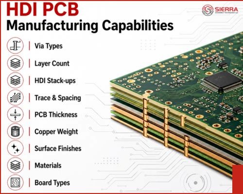
HDI PCB Manufacturing Capabilities
We offer a wide range of HDI PCB fabrication and assembly capabilities designed to support complex, high-performance electronic designs.
Core Capabilities
|
Feature
|
Capability
|
|
Via Types
|
Microvias, blind vias, buried vias, and through-hole vias
|
|
Layer Count
|
Multilayer HDI PCB designs (low to high layer count)
|
|
HDI Stack-ups
|
Standard and advanced HDI build-up structures (1+N+1, 2+N+2, etc.)
|
|
Trace & spacing
|
Fine line and spacing for high-density circuit routing
|
|
PCB Thickness
|
Flexible thickness options based on application needs
|
|
Copper Weight
|
Standard and heavy copper options available
|
|
Surface Finishes
|
ENIG, HASL, OSP, immersion silver, immersion tin
|
|
Materials
|
FR-4, high-Tg materials, and advanced laminates
|
|
Board Types
|
Rigid, flex, and rigid-flex HDI PCBs
|
Advanced HDI Capabilities
Need support for complex, high-performance designs? Our advanced HDI PCB fabrication and assembly capabilities are built to handle even the most demanding applications.
-
Microvia Technology
We use laser-drilled microvias to enable compact, high-density circuit designs with improved performance and reliability.
-
Blind & Buried Vias
Ideal for complex multilayer routing, helping you reduce board size while maintaining functionality.
-
Sequential Lamination
multi-stage lamination processes support advanced HDI structures and precise layer build-up.
-
Controlled Impedance
Designed for high-speed and signal-sensitive applications where performance and accuracy are critical.
-
HDI PCB Prototype
Fast-turn prototyping services help you validate designs quickly and reduce development risks.
-
HDI PCB Assembly
Full assembly support including SMT, thru-hole, and mixed technology for complete flexibility.
-
Testing & Inspection
Comprehensive quality checks including electrical testing and X-ray inspection ensure reliable performance.
-
Custom Design Support
Our engineering team works with you to optimize your design for manufacturability, performance, and cost.
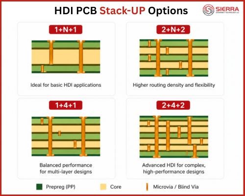
HDI PCB Stack-up Structures
Different HDI PCB stack-up structures allow you to optimize layer count, routing efficiency, and overall board performance. Whether you're working on compact devices or complex multilayer designs, choosing the right stack-up can significantly impact reliability and cost.
-
Better space utilization for compact designs
-
Improved signal integrity in high-speed applications
-
Flexible routing options for complex layouts
-
Optimized performance and manufacturability
Our team helps you select the right stack-up based on your design requirements, ensuring your HDI PCB fabrication and assembly process is efficient and cost-effective.

What Is a High-Density Interconnect PCB?
A high-density interconnect PCB (HDI PCB) is designed to handle more components in less space using advanced technologies like microvias, fine lines, and multilayer stack-ups.
-
Smaller, lighter products
-
Better signal integrity
-
Reduced EMI and signal loss
-
Higher reliability for complex applications
Industries We Serve
|
Core Industries
|
Applications
|
|
Aerospace & Satellite
|
IoT, Smart Home, Wearables
|
|
Defense
|
Security, Wireless Systems
|
|
Medical
|
Video Devices, Healthcare Equipment
|
|
Automotive
|
Bluetooth, Connected Vehicles
|
|
Industrial Electronics
|
Automation, LED Industry
|
|
Consumer Electronics
|
Cameras, Smart Devices
|
|
Telecommunications
|
Business & Computing Systems
|
|
Agricultural
|
Specialized Electronic Systems
|
Advantages of HDI PCB
Why are more engineers choosing high density interconnect PCBs for modern designs?
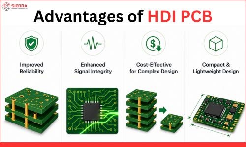
-
Improved Reliability – Microvias reduce stress and enhance durability
-
Enhanced Signal Integrity – Shorter paths improve performance and reduce interference
-
Cost-Effective for Complex Designs – Fewer layers and optimized design lower overall cost
-
Compact & Lightweight Design – More components in less space for smaller devices
Why Engineers and Decision-Makers Choose Sierra
Still comparing options? Here’s why companies trust us as their HDI PCB manufacturer:
-
30+ years of industry experience
-
Advanced US-based manufacturing
-
AS9100 Rev-D & ISO 9001:2015 certified processes
-
IPC-CC-830B compliant standards
-
RoHS compliant assemblies
-
Fast-turn HDI PCB prototypes
-
Scalable production capabilities
-
Dedicated engineering support
Frequently Asked Questions (FAQs)
1. How do I choose the right HDI PCB manufacturer for my project?
Ans: Choosing the right HDI PCB manufacturer depends on experience, certifications, manufacturing capabilities, and turnaround time. You should look for a partner that offers complete HDI PCB fabrication and assembly, supports complex designs, and provides engineering assistance to reduce risks and costs.
2. What is the typical turnaround time for HDI PCB fabrication and assembly?
Ans: Turnaround time depends on design complexity, layer count, and volume. However, most manufacturers offer quick-turn HDI PCB prototype services within a few days, while full production runs may take longer. Fast and reliable delivery is critical for meeting project deadlines.
3. How can I reduce HDI PCB cost without affecting quality?
Ans: You can optimize HDI PCB cost by simplifying the design, reducing unnecessary layers, and working with an experienced manufacturer who can suggest design improvements. Early design validation through HDI PCB prototypes also helps avoid costly errors during production.
4. What industries use high density interconnect PCBs?
Ans: High density interconnect PCBs are widely used in industries that require compact and high-performance electronics, including aerospace, medical devices, automotive, telecommunications, and consumer electronics.
5. Do you provide both HDI PCB fabrication and assembly services?
Ans: Yes, a full-service HDI PCB manufacturer typically offers both HDI PCB fabrication and HDI PCB assembly, along with testing and inspection. This ensures better quality control, faster turnaround, and a streamlined manufacturing process.
Start your HDI PCB project today request a quote now and get expert support, fast turnaround, and certified quality you can trust.